Why is it called as direct coupling?
- The output of the first stage is connected to input of the second stage without any coupling device therefore it is called as direct coupling amplifier.
Circuit Diagram
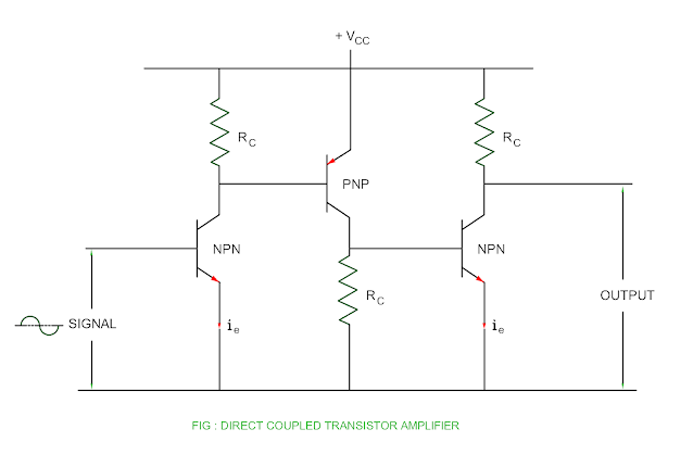
- The circuit diagram of three stage direct coupled amplifier is shown in the Figure.
- It consists of three back to back connections of NPN transistor and PNP transistor.
- The collector output of the first NPN transistor is connected to the input of the PNP transistor.
- Similarly the collector output of the PNP transistor is connected to the input of the NPN transistor.
- The coupling transformer and capacitor is not used at the output otherwise the amplifier becomes bulky at low frequencies.
- The weak ac signal is applied at the base of the NPN transistor, this signal is amplified and output is available at the collector terminal of the NPN transistor.
- The amplified output voltage is available at the base of the PNP transistor.
- The output of the PNP transistor is available at the collector load.
Advantages
- Circuit design is very simple because it requires minimum use of resistors
- Low cost due to absence of coupling capacitor and coupling transformer
Disadvantages
- The operating point may be shifted due to temperature variations which lead to distortion in the output waveform
- This amplifier cannot be used for high frequencies applications.
Applications
- Low frequencies applications such as photo electric current, thermal electrical current
You may also like :
Compare – Voltage harmonics and Current harmonics


No comments:
Post a Comment