Faithful Amplification
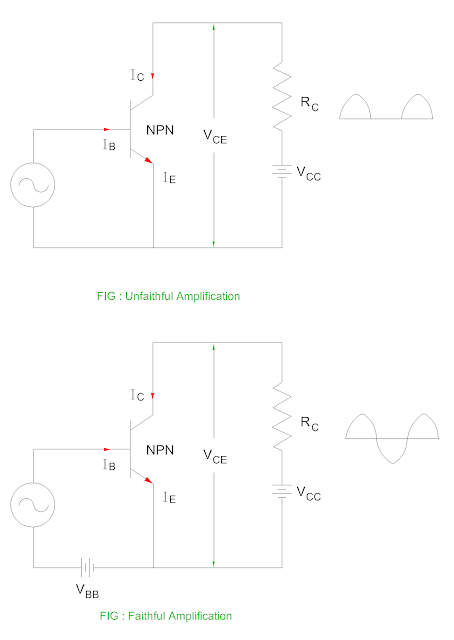
- The raising of strength of input weak signal is called as amplification. The faithful amplification means amplification without change in shape ( output voltage ).
The transistor input circuit remains in forward biased
and output circuit remains in reverse biased during all part of the signal.
Condition for faithful amplification
( 1 ) Proper zero signal collector current
Positive half cycle
- Let us consider the case of NPN transistor as shown in the Figure.
- The base is positive with respect to emitter during positive half cycle of the input supply therefore it becomes forward biased therefore the base current flows resulting the collector current also flows.
Negative half cycle
- The base is negative with respect to emitter during negative half cycle of the input supply therefore it becomes reverse biased resulting no base current flows in the circuit.
- This will result in no output during negative half cycle. This is called as unfaithful amplification.
Function of battery voltage VBB
- The faithful amplification of the transistor is done by introduce DC battery VBB at the input side.
- The magnitude of this DC battery voltage is such that input circuit always in the forward biased even during negative half cycle of the supply.
Zero Signal Collector Current
Signal means AC supply
- The zero signals means no input AC signal. The collector current flows during no signal condition are called as zero signal collector current.
The zero signal collector current ≥ Greater than
maximum collector current due to signal
( Why zero signal collector current always greater
than or equal to maximum collector current due to AC signal only? )
- Let us consider that when the signal is applied to the base of the transistor, peak collector current of 5 mA flows through circuit.
- The zero signal collector current must be at least 5 mA so even during negative half cycle of input supply , no cut off in the waveform.
- If the zero signal collector current is less than 5 mA, there will be cut off in the output.
Current flows during Amplification
- The input circuit is more forward biased during positive half cycle of the input supply therefore the collector current increases.
- The input circuit is less forward biased during negative half cycle of the input supply therefore less collector current flows.
( 2 ) Minimum proper base to emitter voltage at any
instant
- The base to emitter voltage must be greater than 0.5 V for germanium transistor and 0.7 V for silicon transistor.
- If the voltage increases beyond this potential barrier voltage, the current sharply increases.
- If the base to emitter voltage decreases beyond potential barrier voltage of any part of signal, it will result in unfaithful amplification.
( 3 ) Minimum proper collector to emitter voltage at
any instant
- The collector to emitter voltage should not fall below 0.5 V for germanium and 1.0 V for silicon transistor for faithful amplification.
- If the voltage fall below this voltage level, the collector to emitter is not properly reverse biased therefore the collector current cannot attract the charge carrier emitted by emitter.
- This will result in major current flows through base circuit and collector current decreases.
As IC = βIB
- Therefore the current amplification factor β decreases. This will result in unfaithful amplification.
- The collector to emitter voltage should not fall below 0.5 V for germanium and 1.0 V for silicon transistor in order to achieve faithful amplification.
You may also like :


No comments:
Post a Comment