- The main drawback of the SCR is that once it turns on, it will be not turned off in spite of gate signal removes.
- The GTO is upgrade version of the SCR in which it is turned off by negative pulse however the turn off current gain ratio is 4 – 5. ( If the anode current is 200 Amp then turn off current must be is in the range of 200/4 to 200/5 )
Structure
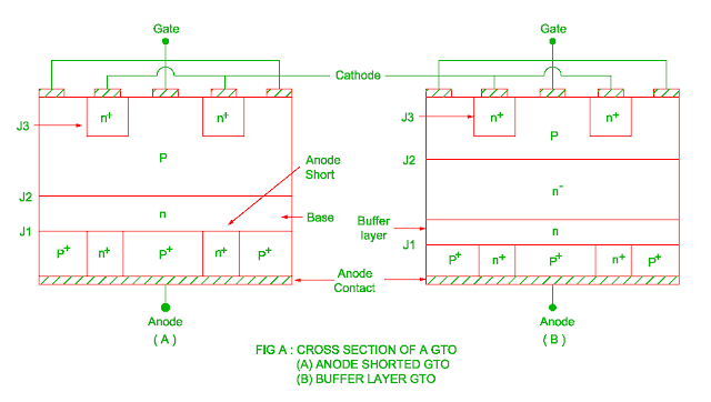
- The structure of the IGBT is similar to that of the SCR. It consists of three junctions and four layer.
n+
Layer
- The n+ doping layer is added near cathode junction in order to increase the efficiency of emitter.
- However the breakdown voltage of the junction J3 reduces up to 20 – 30 V due to this doping level.
P type
gate layer
- There is separate doping level in the P type gate region.
- The doping level of this region must be kept low in order to increase emitter efficiency.
- However the turn off time of the GTO should be kept low by keeping resistivity of this layer minimum which is possible only by high doping level.
- Therefore the doping level of this region must be kept optimum.
- The good turn off capacity of the GTO is possible only when gate – cathode junction is highly inter – digitated. i.e. 2000 amp capacity GTO there are 2000 cathode segments are connected to common point.
N base
region
- The maximum forward blocking voltage depends upon doping and width of the n type base layer.
- If the doping level is kept low and width is kept high, the forward blocking voltage is in the range of kV.
- If the anode voltage increases beyond forward breakdown voltage, the avalanche breakdown occurs.
Anode
junction
- The junction between P+ anode and n base is called as anode junction.
- The doping level of the P+ anode region is kept high in order to increase the anode junction efficiency resulting good turn on characteristics is achieved.
- But it will results in high turn off time and high power losses.
Solve the above
problem
- (a) n+ doping level is added in the P+ anode layer. This is called as the ‘anode shorted GTO structure’. Due to this type of structure (1) Reverse blocking capacity is reduced and (2) Turn on performance is degraded. The density of the anode short is determined in order to keep in mind turn on performance and reverse blocking capacity.
- (b) The n buffer layer is added between anode and n- base layer.
Principal of operation
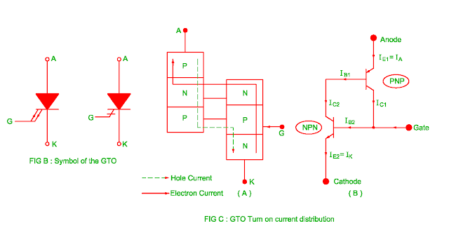
- In the PNP transistor
IC1 = α1IE1
+ ICBO1
IE1 = IA
IC1 = α1IA
+ ICBO1…………(1)
- In the NPN transistor
IC2 = α2IE2
+ ICBO2
IE2 = IK
IC2 = α2IK
+ ICBO2……...…..(2)
- As shown in the Figure B
IK = IA + IG ……….…………(3)
and
IA = IB1 +
IC1 ….…….….(4)
- From equation (2) and (3)
IC2 = α2
( IA + IG ) + ICBO2
IC2 = IB1
= α2 IA + α2 IG
+ ICBO2………(5)
- Now using equation (1) and (5) in the equation (4)
= ( α2 IA + α2 IG + ICBO2 ) + ( α1IA + ICBO1 )
= (α1
+ α2 ) IA + α2 IG + ICBO2+ ICBO1
IA ( 1 – α1 – α2 ) = α2 IG + ICBO2+ ICBO1
IA = ( α2 IG + ICBO2+ ICBO1 ) / (1 –
α1 – α2 )
α1 = Current amplification factor ( PNP
transistor )
α2 = Current amplification factor ( NPN
transistor )
Turn on process
- When the forward voltage is less than the break over voltage, I CBO1 and I CBO2 have small value.
- If the gate current is zero, value of Ia is slightly greater than ( I CBO1 + I CBO2 ). In both conditions ( α1 + α2 ) << 1, therefore the device is called in forward blocking mode.
- The forward voltage is increased or positive gate pulse is injected at gate terminal in order to turn on the GTO.
- As the emitter current increases, the current amplification factor α1 and α2 also increases resulting GTO is turned on.
- When positive gate pulse is injected, ( α1 + α2 ) approaches towards unity and anode current rises sharply.
- This will results in both transistor comes into saturation region and in short time all junction becomes forward biased.
- The voltage drop across the device is equal to voltage drop across any one PN juction.
- Once the device on, it will be turned off only when the anode current reduced below holding current.
Turn off process
- The gate is made negative with respect to cathode in order to turn off the device.
- The holes which are injected from anode is extracted from the gate.
- When gate is made negative with respect to cathode, the junction J3 between P base and N emitter of the NPN transistor is reverse biased resulting electron injection stop.
- This process will extend from P base region to the N emitter region.
- This will result in anode current extend from very far away from gate terminal in the form of filaments so temperature of this region increases.
- If these filaments do not disappear very rapidly the device may be damaged. When this filaments disappears, the process of electron injection stop and depletion layer becomes across junction J2 and J3.
- At this time cathode current almost becomes zero but gate current continue to flow. When the n base carriers reduces, the anode to gate current ‘ tail current’ reduces exponentially.
- Once tail current reduces to zero, the device comes in blocking state. The anode short provides alternative path for tail current.
Static characteristics
- The static characteristics of the GTO are similar to SCR in the first quadrant.
- The latching current in the GTO is much higher than that of SCR for the same rating.
- The forward leakage current in the GTO is much higher than that of the SCR.
- The forward blocking voltage of the GTO is reduced by inserting resistance is in the gate - cathode circuit.
Difference between gold doped GTO and anode shorted GTO
Gold doped GTO
- Higher on state voltage drop
- Higher reverse voltage blocking capacity
- High frequency operation
Anode shorted GTO
- Low on state voltage drop
- Low reverse voltage blocking capacity
- Low frequency operation
You may also like :


