- The power circuit diagram for the single phase half bridge inverter is shown in the figure A.
- The SCR triggering circuit and commutation circuit is not shown for simplicity.
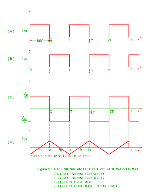
- The SCR T1 is turned on for time 0 ≤ t ≤ T/2 times. This is shown in the figure C.
- The load receives Vdc / 2 voltage from upper DC voltage source. The SCR T1 is turned off and SCR T2 is turned on at time t = T/2.
- The load receives – Vdc / 2 voltage from lower half supply source during time T/2 ≤ t ≤ T time.
- Each SCR gate receives gate pulse at frequency f = 1/T.
- There is 1800 phase displacement between two SCR gate signals.
- The frequency of the output voltage is equal to 1/T and it is controlled by time period T.


