IGBT
- The BJT has low power loss but large turn off time therefore the
switching speed of the IGBT is slow.
- The MOSFET has higher power loss due to
high on state resistance but small turn off time therefore the switching speed
of the MOSFET is high.
- The IGBT has combine characteristics of IGBT and MOSFET.
- The configuration of IGBT consists of BJT and MOSFET in the Darlington
configuration.
- The input of the IGBT consists of MOSFET whereas the output
consists of BJT.
- As the current gain of the BJT has low, the voltage rating of
the MOSFET should be high for higher power rating.
- The input characteristics of
the IGBT should be similar to that of power MOSFET whereas the output
characteristics similar to that of BJT.
Full Form of IGBT
The full form of IGBT is insulated gate bipolar transistor
Structure of IGBT
Why vertical structure?
- The basic structure of the IGBT is shown in
the figure A.
- The structure of the IGBT should be vertical in order to provide
maximum area for flow of current.
- As the on-state resistance decreases, the
power loss also reduces.
Types of IGBT
When we compare the structure of the IGBT with
N- channel MOSFET there is additional P+ layer substrate over N+ layer. This
layer makes PN junction diode with drift layer, this layer is called as inject
layer because it injects holes in the n- layer. There are two types of
impurities in the n type drift layer.
Non-Punch Through IGBT
- It consists of Lightly doped n- layer. It is also called as drift layer.
- The forward blocking voltage in the IGTB depends upon this layer’s doping level
and width.
- It does not affect on state voltage drop due to conductivity modulation.
Punch Through IGBT
- It consists of heavily doped n+ layer.
- It is not necessary for the
operation of this layer.
- It lies between P+ layer and n- layer.
- The on-state
voltage drop, turn off time and also reverse voltage blocking capacity reduces
due to this layer
Symbol and Equivalent Circuit of IGBT
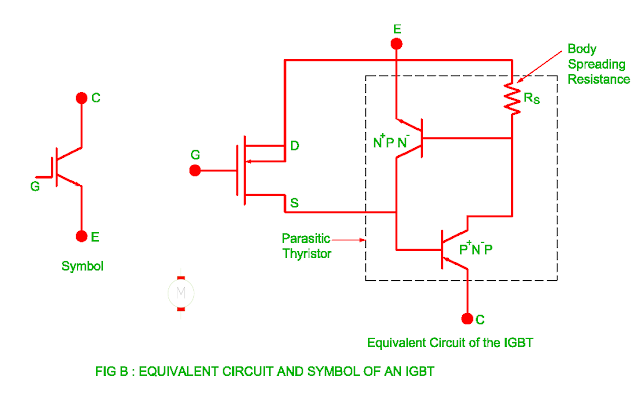
- It consists of three terminals namely collector, emitter and gate.
- The
one cell of IGBT consists of PNP transistor, NPN transistor and driver MOSFET.
PNP transistor
- P+ injecting layer as emitter
- N- drift layer as base
- P body layer as collector
NPN transistor
- N+ region emitter
- P body layer base
- N- drift layer collector
Body Spreading Resistance
- In the NPN transistor base is shorted with emitter but due to lower
quality of short, resistance between emitter and base is called body spreading
resistance.
- If the output current is high, due to high voltage drop across body
spreading resistance and PNPN latching process IGBT turns on.
- The parasitic
thyristor is used to solve problem of latching in which doping of the body
layer is changed.
Operation of IGBT
- The operation of the IGBT is explained as follows
(A) Inversion layer
OFF State
- When gate-emitter voltage less than the threshold voltage, inversion
layer is not created.
- The forward
voltage between collector to emitter reverse biased across junction j2 and only
leakage current flow
ON State
- When gate- emitter voltage greater than threshold voltage inversion
layer is created.
- Due to this inversion layer conduction channel N+NN- is
created, therefore flow of current is possible.
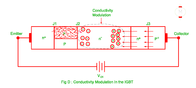
(B) Conducting Modulation
- When forward voltage is given to collector to emitter, junction j3
becomes forward biased therefore holes from P+ layer moves towards n+ buffer
layer.
- The conducting channel is created due to inversion layer resulting there
is creation of space charge region in the n- drift layer.
- Therefore holes are
attracted from n+ buffer layer.
- The double injection takes place (holes from
left and electrons from right) in the n- drift layer therefore its conductivity
increases and resistance is decreased.
- Therefore due to conducting modulation
on state voltage drop across device is reduced.
Latching problem
- The drift region (electric field or movement of charge) of the IGBT
works as a base of the PNP transistor .
- The current gain of the transistor
depends upon the width and doping level of the transistor.
- If this current gain
is kept low, most of the current flow through MOSFET resulting voltage drop
across body spreading resistance is decreased and latching problem is solved.
Static Characteristics of IGBT
The static characteristics of the IGBT is similar to BJT. The
controlling parameter in the BJT is base current whereas gate to emitter
voltage in the IGBT.
Cut off Region
- When the gate-emitter voltage is less than the threshold voltage, the
collector to emitter voltage is equal to supply voltage and it is called as cut
off region.
- The semiconductor device which can withstand forward voltage
between collector to emitter is called as forward breaker over voltage BVCE.
- Its value depends upon avalanche breakdown voltage (high reverse voltage across
the junction, it is moderately operated) of the body – drain PN junction diode
and only leakage current flows through the device.
- The forward breakdown
voltage depends upon collector current in the IGBT.
Active Region
- When the gate- emitter voltage greater than the threshold voltage, the
IGBT operates in the active region.
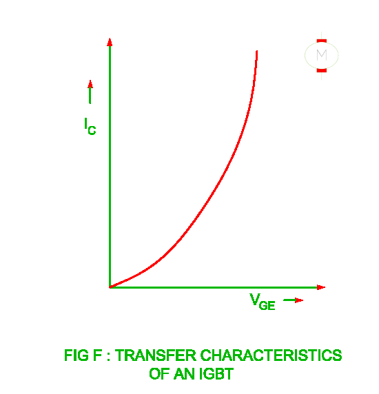
- The collector current depends upon transfer
characteristics of the IGBT. As the gate – emitter voltage increases, the collector
current also increases.
- The characteristics becomes linear for higher value of
collector current.
- The ratio of collector current to the gate – emitter voltage
is called as forward transconductance.
- Forward transconductance: Ic / Vge Mho
Saturation Region
- When the gate - emitter voltage increases, the collector current also
increases as shown in the transfer characteristics of the IGBT.
- The collector to emitter voltage decreases for
a given load resistance RL.
- The collector – emitter voltage ( VCE
) becomes less than the gate – emitter voltage ( VGE ) for a given
specific collector current therefore the MOSFET enter in the ohmic region and P+N-P
transistor in the saturation region. This is called as saturation region of the
device.
- The voltage drop across device becomes constant in this region and this
voltage drop decreases as the gate – emitter voltage ( VGE )
increases.
- The secondary breakdown does not occur in the IGBT as that of in the
BJT. The reverse voltage blocking capability of the punch through IGBT ( PT
IGBT ) is in tens of volt due to heavily doped n+ layer.
- The Non
punch through IGBT ( NPT IGBT ) can withstand maximum reverse voltage VRB.
The IGBT always operate in the saturation or cut off region.
Applications of IGBT
- UPS
- Motor controllers
- Choppers
- Inverters
- SMPS
You may also like to read these articles:
Law of conservation of
Energy
Single Excited System –
Doubly Excited System
How voltage is built up
in Generator?
Armature Reaction in the DC
Generator
Current harmonic –
Voltage harmonic

